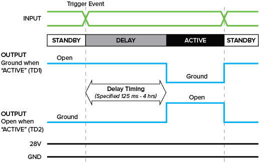
The NEXSYS Time Delay is a Series A (4 pin) device that detects a signal level state change as the event which triggers the delay timer to start. The Time Delay also has the option to start the delay timer upon power-up.
28V: Operating voltage (nom.), 4 mA current draw (max.). Device can be specified to start delay timer on power-up.
GND: Continuous Ground required.
INPUT: The INPUT level determines if the device is in STANDBY or DELAY/ACTIVE mode. The device can be specified to transition to DELAY/ACTIVE mode by an INPUT level state change. The INPUT level state options include +28 VDC, High Impedance, and Ground. INPUT is unused when device is specified as a power-up delay timer.
OUTPUT: The Time Delay offers two output options, based on the state of the OUTPUT signal when ACTIVE. The specified delay timing options range from 125 ms to 4 hours. The output load capacity is 0.5 A (Resistive).
Time Delay (TD1): Ground when ACTIVE and High Impedance when in STANDBY or DELAY.
Time Delay (TD2): High Impedance when ACTIVE and Ground when in STANDBY or DELAY.
To help system designers understand the potential of NEXSYS Component Technology, we have assembled a collection of Application Notes. The links below show example applications that utilize the Time Delay component.
System Soft Power Startup
 This application diagram depicts a power distribution control system with a staggered startup using incremental time delay components. The custom sequential startup pattern ensures that certain units are powered up before others and protects power supplies from transient spikes.